- 您现在的位置:买卖IC网 > Sheet目录3890 > PIC16C765T-I/L (Microchip Technology)IC MCU OTP 8KX14 USB 44PLCC
2000 Microchip Technology Inc.
Preliminary
DS41124C-page 19
PIC16C745/765
Bank 2
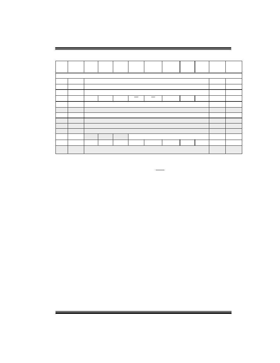
100h
INDF(3)
Addressing this location uses contents of FSR to address data memory (not a physical register)
0000 0000
101h
TMR0
Timer0 module’s register
xxxx xxxx
uuuu uuuu
102h
PCL(3)
Program Counter's (PC) Least Significant Byte
0000 0000
103h
STATUS(3)
IRP
RP1
RP0
TO
PD
ZDC
C
0001 1xxx
000q quuu
104h
FSR(3)
Indirect data memory address pointer
xxxx xxxx
uuuu uuuu
105h
—
Unimplemented
—
106h
PORTB
PORTB Data Latch when written: PORTB pins when read
xxxx xxxx
uuuu uuuu
107h
—
Unimplemented
—
108h
—
Unimplemented
—
109h
—
Unimplemented
—
10Ah
PCLATH(1,3)
—
Write Buffer for the upper 5 bits of the Program Counter
---0 0000
10Bh
INTCON(3)
GIE
PEIE
T0IE
INTE
RBIE
T0IF
INTF
RBIF
0000 000x
0000 000u
10Ch-
11Fh
—
Unimplemented
—
TABLE 4-1:
SPECIAL FUNCTION REGISTER SUMMARY (CONTINUED)
Address
Name
Bit 7
Bit 6
Bit 5
Bit 4
Bit 3
Bit 2
Bit 1
Bit 0
Value on:
POR,
BOR
Value on all
other resets
(2)
Legend: x = unknown, u = unchanged, q = value depends on condition, - = unimplemented read as ’0’.
Shaded locations are unimplemented, read as ‘0’.
Note 1:
The upper byte of the program counter is not directly accessible. PCLATH is a holding register for the PC<12:8> whose contents
are transferred to the upper byte of the program counter.
2:
Other (non power-up) RESETS include external RESET through MCLR and Watchdog Timer Reset.
3:
These registers can be addressed from any bank.
4:
The Parallel Slave Port (PORTD and PORTE) is not implemented on the PIC16C745, always maintain these bits clear.
745cov.book Page 19 Wednesday, August 2, 2000 8:24 AM
发布紧急采购,3分钟左右您将得到回复。
相关PDF资料
PIC18C442T-E/L
IC MCU OTP 8KX16 A/D 44PLCC
PIC16C621A-40/SS
IC MCU OTP 1KX14 COMP 20SSOP
PIC16C622A-40/SS
IC MCU OTP 2KX14 COMP 20SSOP
PIC16CE623-30/SO
IC MCU OTP 512X14 EE COMP 18SOIC
PIC16CE624-30/SO
IC MCU OTP 1KX14 EE COMP 18SOIC
PIC16CE624-30/SS
IC MCU OTP 1KX14 EE COMP 20SSOP
PIC16CE623-30/SS
IC MCU OTP 512X14 EE COMP 20SSOP
PIC16CE624-30/P
IC MCU OTP 1KX14 EE COMP 18DIP
相关代理商/技术参数
PIC16C765T-I/PT
功能描述:8位微控制器 -MCU 14KB 256 RAM 33 I/O RoHS:否 制造商:Silicon Labs 核心:8051 处理器系列:C8051F39x 数据总线宽度:8 bit 最大时钟频率:50 MHz 程序存储器大小:16 KB 数据 RAM 大小:1 KB 片上 ADC:Yes 工作电源电压:1.8 V to 3.6 V 工作温度范围:- 40 C to + 105 C 封装 / 箱体:QFN-20 安装风格:SMD/SMT
PIC16C76T-04/SO
功能描述:8位微控制器 -MCU 14KB 368 RAM 22 I/O RoHS:否 制造商:Silicon Labs 核心:8051 处理器系列:C8051F39x 数据总线宽度:8 bit 最大时钟频率:50 MHz 程序存储器大小:16 KB 数据 RAM 大小:1 KB 片上 ADC:Yes 工作电源电压:1.8 V to 3.6 V 工作温度范围:- 40 C to + 105 C 封装 / 箱体:QFN-20 安装风格:SMD/SMT
PIC16C76T-04E/SO
功能描述:8位微控制器 -MCU 14KB 368 RAM 22 I/O RoHS:否 制造商:Silicon Labs 核心:8051 处理器系列:C8051F39x 数据总线宽度:8 bit 最大时钟频率:50 MHz 程序存储器大小:16 KB 数据 RAM 大小:1 KB 片上 ADC:Yes 工作电源电压:1.8 V to 3.6 V 工作温度范围:- 40 C to + 105 C 封装 / 箱体:QFN-20 安装风格:SMD/SMT
PIC16C76T-04I/SO
功能描述:8位微控制器 -MCU 14KB 368 RAM 22 I/O RoHS:否 制造商:Silicon Labs 核心:8051 处理器系列:C8051F39x 数据总线宽度:8 bit 最大时钟频率:50 MHz 程序存储器大小:16 KB 数据 RAM 大小:1 KB 片上 ADC:Yes 工作电源电压:1.8 V to 3.6 V 工作温度范围:- 40 C to + 105 C 封装 / 箱体:QFN-20 安装风格:SMD/SMT
PIC16C76T-10/SO
功能描述:8位微控制器 -MCU 14KB 368 RAM 22 I/O RoHS:否 制造商:Silicon Labs 核心:8051 处理器系列:C8051F39x 数据总线宽度:8 bit 最大时钟频率:50 MHz 程序存储器大小:16 KB 数据 RAM 大小:1 KB 片上 ADC:Yes 工作电源电压:1.8 V to 3.6 V 工作温度范围:- 40 C to + 105 C 封装 / 箱体:QFN-20 安装风格:SMD/SMT
PIC16C76T-10E/SO
功能描述:8位微控制器 -MCU 14KB 368 RAM 22 I/O RoHS:否 制造商:Silicon Labs 核心:8051 处理器系列:C8051F39x 数据总线宽度:8 bit 最大时钟频率:50 MHz 程序存储器大小:16 KB 数据 RAM 大小:1 KB 片上 ADC:Yes 工作电源电压:1.8 V to 3.6 V 工作温度范围:- 40 C to + 105 C 封装 / 箱体:QFN-20 安装风格:SMD/SMT
PIC16C76T-10I/SO
功能描述:8位微控制器 -MCU 14KB 368 RAM 22 I/O RoHS:否 制造商:Silicon Labs 核心:8051 处理器系列:C8051F39x 数据总线宽度:8 bit 最大时钟频率:50 MHz 程序存储器大小:16 KB 数据 RAM 大小:1 KB 片上 ADC:Yes 工作电源电压:1.8 V to 3.6 V 工作温度范围:- 40 C to + 105 C 封装 / 箱体:QFN-20 安装风格:SMD/SMT
PIC16C76T-20/SO
功能描述:8位微控制器 -MCU 14KB 368 RAM 22 I/O RoHS:否 制造商:Silicon Labs 核心:8051 处理器系列:C8051F39x 数据总线宽度:8 bit 最大时钟频率:50 MHz 程序存储器大小:16 KB 数据 RAM 大小:1 KB 片上 ADC:Yes 工作电源电压:1.8 V to 3.6 V 工作温度范围:- 40 C to + 105 C 封装 / 箱体:QFN-20 安装风格:SMD/SMT